If you know how to train or serve a model on cloud GPUs, the mathematics of device inference will feel familiar. The unfamiliar part is where the work runs, how its data moves, and what else shares the machine.
A phone is not a smaller GPU server. Its CPU, GPU, neural accelerator, camera and audio engines form a coordinated system. A camera, television or robot has a different balance again. The useful question is not “Which chip has the most TOPS?” but “Which complete device can execute my workload, with the required quality, responsiveness and sustained power?”12
This page builds that mental model, then introduces current flagship families and representative specialist platforms. It focuses on inference, not chip design or a buying recommendation. The hardware and software sources were checked October 12, 2026. Vendor specifications are not our measurements; announcements and availability claims are identified separately.
From a cloud GPU to a device system
Think in three layers: execution engines, memory topology and the product envelope. Changing only the first can leave the real bottleneck untouched. Figure 1 compares three useful memory arrangements.
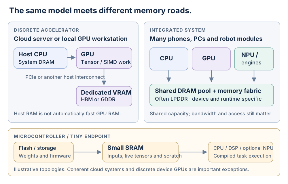
Figure 1. Follow the memory roads. Independent synthesis of CUDA, MLX and embedded platform documentation.345
A conventional discrete GPU server has CPU memory and a separate GPU memory pool. You stage inputs and weights onto the GPU, then try to keep useful work there. An integrated device can let processors access a shared physical pool. MLX, for example, exposes shared arrays to the CPU and GPU on Apple silicon. This can avoid copying the same tensor between separate memory pools, but it does not remove execution dependencies.34
These are topologies, not location rules. A desktop RTX card also has dedicated memory; DGX Spark is a local machine with coherent shared memory. Cloud systems can use coherent CPU and GPU designs as well. “Unified memory” must be read in the context of the hardware and runtime, not treated as a promise of unlimited fast GPU memory.673
What changes when the application moves onto a device
6 dimensions| Dimension | A cloud GPU service often optimizes | A device application must also consider |
|---|---|---|
| Workload | Many requests, batching and service utilization | One interactive user, camera streams or several competing features; batching may add unacceptable delay |
| Memory | GPU capacity, memory traffic and multi-GPU communication | The model shares a budget with the OS, app, display and sensor buffers; allocation limits can be below installed RAM |
| Execution | A selected server architecture and software image | CPU, GPU and NPU placement, driver versions, supported operators and multiple device generations |
| Power and cooling | Facility and accelerator limits under managed cooling | Battery, enclosure, surface temperature and sustained use; a plugged-in TV still has thermal limits |
| Inputs | Requests that have already crossed a network boundary | Capture, timestamps, ISP/DSP processing and evidence that can become stale while inference runs |
| Reliability | Service recovery and fleet observability | Model downloads, offline readiness, interruption, app lifecycle and local fallback |
No matching dimensions. Try another term or reset the search.
Scroll to compare. Focus view gives the table more room.
This is a design comparison, not a claim that cloud systems lack latency or power constraints. It combines mobile runtime, thermal and sensor platform contracts.1258 See Production and product design for the application lifecycle.
Inside a heterogeneous chip
A system on chip, or SoC, integrates several functions behind one system interface. It need not be one silicon die: Apple’s M5 Pro and M5 Max combine two dies in one SoC. A system on module, or SoM, adds a board-level package around a processor, memory and other required components. A developer kit adds a carrier board, connectors and a usable development environment. Jetson distinguishes production modules from developer kits.910
Figure 2 shows the roles, not the floorplan of a particular vendor. An actual device can omit, combine or duplicate these engines.
NPU means neural processing unit, DSP digital signal processor, and ISP image signal processor. The names identify intended roles, not a uniform hardware design or a guarantee of application access.
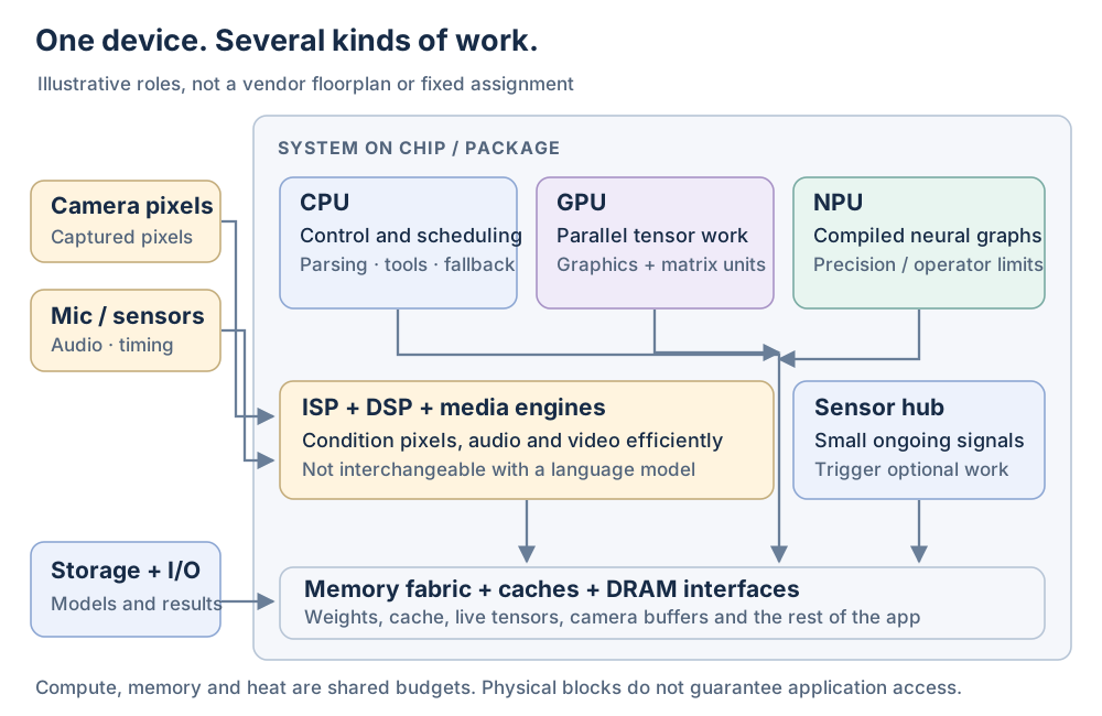
Figure 2. A device is a team of processors. Independent role map informed by CPU/GPU, NPU and sensor platform documentation.1112813
Learn the role before the acronym
6 engine types| Engine | A useful mental model | Typical contribution | Important boundary |
|---|---|---|---|
| CPU | Flexible control plus vector instructions | Tokenization, parsing, scheduling, tools, small kernels and unsupported operations | Not only a fallback; vector or matrix instructions can make some AI work efficient |
| GPU | Programmable parallel throughput | Large matrix work, image models, decoding kernels, graphics and some local training | Many GPUs already contain specialized matrix units; compute competes with graphics and memory traffic |
| NPU | A neural graph accelerator | Supported tensor operations executed through a compiler and runtime | Its operator, precision, shape and driver contract matters more than the name “NPU” |
| DSP | Efficient signal and vector processing | Audio conditioning, sensor processing and some neural operations | Can coexist with or form part of a vendor’s AI accelerator; not every chip exposes a separate DSP |
| ISP and media engines | Specialized pixel and video machinery | Camera conditioning, image processing, video encode and decode | These are not general substitutes for an LLM or an arbitrary vision network |
| Sensor hub / microcontroller | A small ongoing control domain | Capture timing, low duty-cycle signals, triggers and control | A trigger can wake heavier processing; safety and timing require their own system design |
No matching engine types. Try another term or reset the search.
Scroll to compare. Focus view gives the table more room.
The role map is a synthesis, not a mandatory allocation rule. CUDA describes the CPU/GPU control-versus-throughput distinction; Arm’s Ethos range and the QNN and OpenVINO interfaces show why NPU execution is a separate software contract. NXP, ST and Qualcomm expose concrete sensor and control domains. An engine’s existence does not prove that your app can program it directly.111214158513
GPU matrix units are not the same thing as a separate NPU
Modern GPU arithmetic includes specialized matrix hardware. RTX 5090 has Tensor Cores; M5 GPUs have Neural Accelerators in their GPU cores; Snapdragon 8 Elite Extreme Gen 6 lists Adreno matrix cores alongside its Hexagon NPU. The word “neural” therefore does not identify a single execution path.6913
On a Mac, MLX’s shared-array CPU/GPU path is not an Apple Neural Engine backend. Core ML separately lets an application allow CPU, GPU and Neural Engine combinations, with the OS selecting among permitted compute units. Allowing an engine is not a guarantee that the entire model runs on it.416
Memory often decides the feasible model
Separate four quantities: stored weights, working capacity, memory bandwidth and data layout. A checkpoint can fit on disk but fail in working memory. Shared DRAM can improve capacity flexibility while remaining a bandwidth bottleneck. Small on-chip caches or SRAM are faster working spaces, not permission to keep the whole model there.145
HBM, GDDR and LPDDR are DRAM families, not model formats. In the examples here, HBM serves the cloud accelerator, GDDR the discrete graphics card, and LPDDR integrated PC and embedded platforms. The memory name alone does not establish capacity or attainable bandwidth.1761819
For a bus making transfers per second across data bits, the theoretical payload bandwidth is:
This is bus-width arithmetic, not attained application bandwidth. Snapdragon X2 Elite’s published 9,523 MT/s and 128-bit memory interface gives approximately 152.4 GB/s, consistent with its rounded 152 GB/s specification. Different SKUs also list 192-bit interfaces and 228 GB/s. Do not convert an MT/s rating as if it were a separate clock to double again.18
To see why capacity and bandwidth are different, compare Apple’s published M5 Max maximum of 128 GB and 614 GB/s with H200’s 141 GB and 4.8 TB/s. Their capacities are in the same broad range, but their memory paths and system envelopes are not. H200 is a cloud reference example here, not a claim that it is the newest data-center chip.917
For a hypothetical decoder that reads 4 GB of packed weights per accepted token at an effective 100 GB/s, the traffic bound is:
That is 40 ms, or at most 25 tokens/s from weight traffic alone under this one-sweep, one-token-per-step premise. Cache reads, arithmetic, unpacking and synchronization remain; overlap, batching and multi-token verification can change the premise. This is our illustrative calculation, not a chip benchmark. Foundations and Efficient inference develop these bounds.
Shared memory does not mean zero boundary cost
Sharing physical DRAM can avoid a copy between separate pools. It does not guarantee that CPU, GPU and NPU can consume the same buffer format without conversion, synchronization or a driver-managed copy. Google’s LiteRT guide warns that split GPU/CPU graphs can be slower than CPU-only execution because of synchronization. Keep the tensor on a compatible path, not just on the same motherboard.420
The installed RAM is also not an app reservation. Retain space for the KV cache, activations, compiler/runtime workspace, OS and sensor buffers. Budget the allocations that coexist. See peak memory lifetimes.
Read performance labels without being misled
TOPS means trillions of operations per second; TFLOPS counts floating point operations. GOPS uses billions rather than trillions: 600 GOPS is 0.6 TOPS only under the same operation-counting convention. None of these labels tells you how many useful tasks finish. Read the precision, sparsity rule, included engines and power mode beside the number.
The ambiguity is concrete: Hailo’s same 10H module lists 40 TOPS at INT4 and 20 TOPS at INT8. NVIDIA lists T5000’s 2,070 TFLOPS as sparse FP4, while Orin Nano’s 67 TOPS is sparse INT8. Those figures are not one comparable performance axis.211910
Six questions for any chip specification
6 checks| Label | What to ask | What it does not establish |
|---|---|---|
| Precision | INT4, INT8, FP16, BF16 or FP4? What is the accumulation format? | That a four-bit checkpoint uses every operation at four bits |
| Sparsity | Dense work or an assumed supported sparsity pattern? | That ordinary dense weights reach the advertised sparse rate |
| Engine scope | NPU alone, GPU alone or a sum across the platform? | That one indivisible graph can exploit the sum simultaneously |
| Shape | Which batch, sequence length, convolution or matrix dimensions? | That peak utilization holds for batch-one decoding or small kernels |
| Memory | Capacity, theoretical bandwidth and actual tensor traffic? | That stored size predicts runtime peak or effective bandwidth |
| Power | Chip TDP, module mode, board power, supply rating or measured energy? | That these are interchangeable or equal to whole-product battery drain |
No matching checks. Try another term or reset the search.
Scroll to compare. Focus view gives the table more room.
This is an editorial inspection checklist grounded in the variant and scope differences above. DGX Spark makes the last distinction especially clear: 140 W GB10 thermal design power (TDP) and a 240 W power supply are different specifications, not two measurements of its workload energy.7
Compression must match the accelerator’s actual arithmetic and packing. An INT4 weight file may use floating point activations or be expanded by a backend. Quantization, supported kernels and retained accuracy must be verified together. Continue with Quantization and compression.
Current chips and device platforms
There is no single state-of-the-art Edge AI chip. A GPU workstation, an always-worn camera and a motor controller optimize different useful capabilities. The following 19 platforms cover current flagship families and established specialist designs, rather than rank them. Search by a device, chip or development term.
Numbers are published maxima or selected variants, not a benchmark. The access column describes inspected evidence: an OEM product listing, a developer platform or a chip integration route. It does not verify worldwide inventory, SDK access for every application, or every listed model on the chip.
Chip explorer · October 2026 evidence snapshot
19 platforms| Platform | Device and role | Published hardware to notice | Availability evidence and development boundary |
|---|---|---|---|
| Apple M5 Pro / M5 Max | PC and mobile workstation; integrated CPU, GPU and Neural Engine | Up to 64 GB / 307 GB/s for Pro; 128 GB / 614 GB/s for Max. GPU Neural Accelerators are distinct from the Neural Engine | MacBook Pro availability from March 11, 2026. Core ML or Metal; MLX targets CPU/GPU.94 |
| Intel Core Ultra Series 3 | PC and embedded systems; CPU, Arc GPU and NPU | Up to 50 NPU TOPS versus about 180 total platform TOPS on selected variants. The cited brochure does not define a comparable precision/sparsity basis for those headline values | Published platform and SKU brochure, not a stock check. OpenVINO exposes distinct CPU/GPU/NPU paths; shapes and drivers remain version-specific.2215 |
| AMD Ryzen AI 400 | PC; x86 CPU, Radeon GPU and XDNA 2 NPU | HX 475 lists 60 NPU TOPS; other SKUs list 50 or 55. Published configurable TDP (cTDP) of 15–54 W is not measured app energy | OEM systems announced for Q1 2026. Ryzen AI Software supplies NPU deployment and separate GPU flows; not every backend is interchangeable.2324 |
| AMD Ryzen AI Max+ 395 / Halo | PC and compact AI workstation; shared-memory Radeon compute | Original Halo configuration uses Max+ 395 and up to 128 GB unified memory | June 2026 preorder announcement. Verify the actual OEM configuration; larger Max PRO 400 variants remain a separately dated announcement below.25 |
| Qualcomm Snapdragon X2 Elite / Extreme | Arm PC; Oryon CPU, Adreno GPU, Hexagon NPU and sensing hub | Current brief lists 80 or 85 INT8 NPU TOPS by SKU and 152 or 228 GB/s memory bandwidth. Installed capacity is device-specific | Published product brief. QNN/AI Engine Direct supplies an accelerator route; verify OS, driver, SKU and supported model format.1814 |
| NVIDIA GeForce RTX 5090 | PC workstation; discrete GPU | 32 GB dedicated GDDR7, Tensor Cores and 575 W total graphics power specification | Product page provides buying options. CUDA ecosystem; host RAM is separate from VRAM. A desktop card’s envelope is not a phone’s.6 |
| NVIDIA GB10 / DGX Spark | Desktop local AI system; Arm CPU and Blackwell GPU | 128 GB coherent memory, 273 GB/s, 140 W GB10 TDP. The newly listed 64 GB OEM option is marked coming soon | 128 GB system has a purchase route. NVIDIA AI stack on DGX OS; the 240 W supply is not workload power.7 |
| Apple A20 Pro | Phone; CPU, GPU, Neural Engine and imaging pipeline | Dual 16-core Neural Engine; packaging and vapor-chamber changes emphasize sustained performance. Neural core count is not a cross-vendor throughput measure | iPhone 18 Pro availability from September 18, 2026. App execution still follows Apple’s supported APIs and resource limits.2616 |
| Snapdragon 8 Elite Gen 6 / Extreme | Phone; Oryon CPU, Adreno GPU, Hexagon NPU and low power sensing | Extreme lists Adreno matrix cores as well as Hexagon NPU and micro NPUs. No common absolute TOPS value is established here | Current product pages inspected; OEM rollout and SDK coverage require their own check. Do not infer an arbitrary model API from an agentic feature promise.13 |
| MediaTek Dimensity 9600 Pro | Phone; integrated generative AI and imaging | NPU 1090 plus Super Efficient NPU 2.0; LPDDR6 and CPU/GPU/ISP integration are listed features | Current flagship product listing. Absolute task performance and app access were not independently established.27 |
| Samsung Exynos 2600 | Phone; CPU, GPU, NPU and imaging | Integrated CPU/NPU/GPU; CPU SME2 matrix instructions and a dedicated thermal packaging feature | Current product listing, not a claim that every regional phone uses it. Check the actual handset and application backend.28 |
| Qualcomm Snapdragon AR1+ Gen 1 | Smart glasses; capture, audio, display and small-model inference | Hexagon NPU and dual ISPs; the vendor demonstrated Llama 1B running on glasses in June 2025 | Platform plus controlled demonstration, not proof that all glasses assistants run entirely locally or expose general model loading.2930 |
| Ambarella CV75S | Camera and compact vision products; CVflow plus imaging/video | Integrated 4KP30+ image/video processing and neural inference. Video format support is not a model FPS benchmark | Published camera SoC listing; CNN toolkit is described, while the detailed product brief requires registration. Primarily an OEM integration route.31 |
| MediaTek Pentonic 800 | TV and smart display; picture processing, audio and video | Integrated AI processor, image enhancement and video decoding; up to 64-bit DDR4 at 3200 Mb/s is listed | Established product listing. Picture-quality AI is not evidence of a freely programmable LLM backend in a retail TV.32 |
| NVIDIA Jetson T5000 / AGX Thor | Robot and high-end sensor system; Blackwell GPU plus Arm CPU | 128 GB LPDDR5X, 273 GB/s, 40–130 W module modes; 2,070 sparse FP4 TFLOPS | General availability announced August 25, 2025. JetPack/CUDA/robotics stack; module mode does not measure whole-robot power.1933 |
| Jetson Orin Nano Super | Compact robot, drone and camera prototype; Ampere GPU | 8 GB LPDDR5 and about 102 GB/s; 67 sparse INT8 TOPS versus about 33 dense INT8 TOPS | Developer kit has a purchase route. Retain exact module, software and power mode; older narrative maxima on the page differ from the updated specification table.10 |
| Hailo-10H / Raspberry Pi AI HAT+ 2 | SBC, camera and small agent system; external accelerator | HAT+ 2 has 8 GB dedicated RAM and 40 INT4 TOPS. The M.2 brief separately lists 40 INT4 / 20 INT8 TOPS and PCIe Gen 3 x4 | Pi 5 add-on marked available now. Use compatible compiled models and Hailo tooling; accelerator RAM is not added to the Pi’s host RAM pool.3421 |
| NXP i.MX 95 | Industrial system and robot controller; application and control domains | Up to six Cortex-A55 cores, Cortex-M7/M33 domains and eIQ Neutron NPU; external LPDDR interface | Active product family and evaluation/module ecosystem. Linux/application inference and real-time control require distinct integration contracts.8 |
| ST STM32N6 | Microcontroller endpoint; local vision, audio and control | Cortex-M55, Neural-ART up to 600 GOPS, 4.2 MB embedded RAM plus external memory interfaces | Available product family. N6x7 AI line has Neural-ART; the GP line does not. This is a tiny compiled-task regime, not a desktop LLM machine.5 |
No matching platforms. Try another term or reset the search.
Scroll to compare. Focus view gives the table more room.
The device column describes target roles, not exclusive categories. A phone chip can appear in an embedded board; an industrial PC can power a robot. The chip, board, cooling, memory configuration and software stack together define the usable platform.
Announced directions, not assumed availability
Keep a roadmap separate from hardware you can test. The inspected announcement is the evidence below; a target date that has passed is not proof of shipment.
Announcements to track separately
3 announcements| Platform | What was announced | Availability boundary |
|---|---|---|
| Jetson T3000 / T2000 | July 15, 2026: lower-tier Thor modules with 32 GB and 16 GB respectively | Modules scheduled for Q1 2027. T5000-kit emulation is a development path, not the physical target board.35 |
| Ryzen AI Max PRO 400 / next Halo | June 2026: next Halo configuration planned with up to 192 GB unified memory and 160 GB described as VRAM | Q3 2026 target in that announcement. Shipment and exact memory-allocation behavior not verified here.25 |
| Snapdragon Reality Elite / XREAL Aura | June 16, 2026: new XR platform and planned optical see-through glasses | Consumer availability was planned for later in 2026. A display/AI platform announcement does not establish unrestricted model access.36 |
No matching announcements. Try another term or reset the search.
Scroll to compare. Focus view gives the table more room.
This distinction matters particularly for research: an emulator, an advertised maximum and a shipping target with stable drivers answer different questions.
The runtime is part of the hardware contract
A PyTorch model is not automatically a program for every device engine. Export, quantization, graph lowering and backend-specific compilation decide which operations can execute. The fallback graph, temporary buffers and initialization work remain part of the application.141524
A map of developer entry points
6 paths| Target | Useful entry point | Check before assuming acceleration |
|---|---|---|
| Apple GPU versus Neural Engine | MLX/Metal for CPU/GPU work; Core ML for supported compute-unit combinations | Model conversion and actual compute placement; MLX does not silently become a Neural Engine backend.416 |
| Qualcomm NPU | AI Engine Direct / QNN, including ONNX Runtime QNN EP | Supported operators, fixed input shapes, precision, driver and SDK. The inspected QNN EP does not accept dynamic shapes or general Loops/Ifs.14 |
| Intel CPU/GPU/NPU | OpenVINO and its per-device plugins | NPU dynamic shapes are a limited preview in the inspected 2026 docs, with bounded vision-model scope, required drivers and compiler mode.15 |
| AMD GPU versus XDNA NPU | GPU frameworks appropriate to supported configurations; Ryzen AI Software for compiled NPU and LLM flows | The current Ryzen AI Software guide separates iGPU llama.cpp from NPU paths; verify the model and execution provider.24 |
| NVIDIA GPU and Jetson | CUDA libraries/frameworks plus the target JetPack stack | Architecture, supported precision, memory capacity and sensor path; server kernels are not automatically tuned for embedded shapes.111910 |
| Camera / TV / MCU | Vendor toolchains, platform APIs and embedded deployment tools | OEM access, memory planning and a supported compiled model; an integrated AI feature is not a public arbitrary-model interface.313212 |
No matching paths. Try another term or reset the search.
Scroll to compare. Focus view gives the table more room.
These are entry points, not installation instructions or promises of universal support. Read Runtimes, compilers and kernels for export and processor-boundary costs.
Match the device to the complete workload
Three examples make the design consequences concrete. They are proposed allocations, not measured implementations.
A local PC document assistant. Capacity and effective bandwidth decide whether the model, visual input and cache coexist comfortably. A GPU path may be easier to experiment with; an NPU path may suit a supported production model. Test prefill and decoding separately rather than choose by NPU TOPS.
Glasses or a camera. Preserve capture timestamps and use inexpensive continuous processing to decide when a larger model should run. Include the ISP/DSP, view selection, radio and response delivery in the energy budget. A phone companion or permitted cloud route may be part of the design; local capture is not proof of local reasoning. Qualcomm’s on-glass demo establishes one small-model configuration, not a universal architecture.30
A robot. Perception, language reasoning, planning and fast control have different deadlines. NXP’s separate application and microcontroller domains illustrate why these can be separated. Our design recommendation is to retain a bounded control and recovery path rather than depend on an unconstrained language response meeting every deadline. A chip’s safety-related feature does not certify the complete robot.8
Figure 3 turns these examples into a repeatable investigation.
- Define the workloadInputs, output quality, deadline and sustained use
- Map engines and memoryInstalled resources, permitted APIs and tensor traffic
- Compile the real artifactPrecision, shapes, supported operators and fallback
- Measure the complete deviceCold/warm latency, peak memory, quality and energy
Compare traces before and after optimization. A changed artifact, driver, cooling mode or context length is a changed experiment.
Figure 3. Close the loop on the actual device. Independent workflow informed by runtime and thermal guidance.1214
Keep the device model, RAM configuration, firmware, OS, driver, runtime, checkpoint, quantization, input shapes, output lengths and power mode in the test record. Measure correctness, first useful result, completion, peak allocation, sustained temperature and energy for the same workload. TDP and a supply rating cannot replace measured joules per useful task.
The most valuable research question is often what representation and execution path preserve the capability within this device’s envelope? Use Efficient models, Multimodal workloads and Evaluation and profiling for the next layer.
References
-
ONNX Runtime. Deploy on mobile, model requirements, execution providers and application measurements. Inspected October 12, 2026. ↩ ↩2 ↩3 ↩4
-
Android Developers. Thermal API, thermal status, headroom and device support; page updated February 26, 2026, inspected October 12. ↩ ↩2 ↩3
-
NVIDIA. CUDA Unified and System Memory, Sections 2.6.1–2.6.2, physical pools, managed migration and hardware coherency. Inspected October 12, 2026. ↩ ↩2 ↩3
-
MLX. Unified Memory, version 0.32.3, CPU/GPU shared-array execution. Inspected October 12, 2026. ↩ ↩2 ↩3 ↩4 ↩5 ↩6 ↩7
-
STMicroelectronics. STM32N6 series, processing, Neural-ART, memory, camera pipeline and AI versus GP product lines. Inspected October 12, 2026. ↩ ↩2 ↩3 ↩4 ↩5
-
NVIDIA. GeForce RTX 5090, Tensor Cores, GDDR7 and thermal/power specifications. Inspected October 12, 2026; performance testimonials and placeholder pricing are not used. ↩ ↩2 ↩3 ↩4
-
NVIDIA. DGX Spark, configurations, purchase/coming-soon distinction, bandwidth and GB10 TDP versus supply rating. Inspected October 12, 2026. ↩ ↩2 ↩3
-
NXP. i.MX 95 applications processors, Features: application/control cores, Neutron NPU, memory and interfaces. Inspected October 12, 2026. ↩ ↩2 ↩3 ↩4 ↩5
-
Apple. M5 Pro and M5 Max, March 3, 2026; Fusion Architecture, maximum memory/bandwidth and March 11 availability. ↩ ↩2 ↩3 ↩4
-
NVIDIA. Jetson Orin, updated module/developer-kit specifications and dense/sparse engine breakdown. Inspected October 12, 2026; the selected Nano Super figures follow the specification table, not older introductory maxima. ↩ ↩2 ↩3 ↩4
-
NVIDIA. CUDA Programming Guide: Introduction, CPU/GPU design goals and programmable throughput; documentation updated September 10, 2026. ↩ ↩2 ↩3
-
Arm. Ethos-U85, NPU role, supported network scope, Cortex-A/M targets and reference-design/toolchain boundary. This is licensable IP, not a retail chip; inspected October 12, 2026. ↩ ↩2 ↩3
-
Qualcomm. Snapdragon 8 Elite Gen 6 and Extreme Gen 6, Features/specifications. Current public product specifications inspected October 12, 2026; relative marketing gains are not benchmark evidence here. ↩ ↩2 ↩3 ↩4
-
ONNX Runtime. QNN Execution Provider, accelerator backends and Model requirements, including fixed shapes and unsupported control-flow operators. Inspected October 12, 2026. ↩ ↩2 ↩3 ↩4 ↩5
-
Intel. OpenVINO NPU device, 2026 documentation, Dynamic Shapes and Limitations. Its bounded dynamic-shape preview is not general dynamic LLM support. ↩ ↩2 ↩3 ↩4
-
Apple. MLComputeUnits, processing-unit combinations and OS selection; official Markdown documentation inspected October 12, 2026. ↩ ↩2 ↩3
-
NVIDIA. H200, HBM3e capacity and bandwidth. Inspected October 12, 2026; included as a familiar cloud memory reference, not a newest-chip ranking. ↩ ↩2
-
Qualcomm. Snapdragon X2 Elite Product Brief, four-page edition inspected October 12, 2026, SKU tables on PDF pages 3–4. INT8 TOPS, interface width, transfer rate, bandwidth and configured capacity remain SKU-specific. ↩ ↩2 ↩3
-
NVIDIA. Jetson Thor, T5000 specifications, sparse FP4 labeling, memory and module power modes. Inspected October 12, 2026; sibling specifications are not assigned to T5000. ↩ ↩2 ↩3 ↩4
-
Google AI Edge. GPU delegates for LiteRT, Troubleshooting GPU support. Inspected October 12, 2026; synchronization cost depends on the actual partitioned graph. ↩
-
Hailo. Hailo-10H M.2 Key M ET product brief, two-page edition, precision-specific peak rates, dedicated memory and PCIe interface. Inspected October 12, 2026. ↩ ↩2
-
Intel. Core Ultra Series 3 for the Edge overview, inspected 26-page edition, PDF pages 15–16. Used for hardware/software structure and scoped maxima, not its vendor performance comparisons or roadmap guarantees. ↩
-
AMD. CES 2026 client announcements, January 5, 2026, Ryzen AI 400 SKU table and OEM availability plan. ↩
-
AMD. Ryzen AI Software, version 1.8.0, updated October 7, 2026; compiled NPU flow and separate iGPU/LLM interfaces. Inspected October 12. ↩ ↩2 ↩3
-
AMD. Ryzen AI Halo and Ryzen AI Max PRO 400 announcement, June 2026; original 395 configuration, preorder plan and separate next-generation memory/availability proposal. A projected date is not verified shipment. ↩ ↩2
-
Apple. iPhone 18 Pro and A20 Pro, September 9, 2026, A20 Pro, thermal management and September 18 availability. ↩
-
MediaTek. Dimensity 9600 Pro, dual NPUs, memory interface and CPU/GPU/ISP architecture. Inspected October 12, 2026; unqualified efficiency and latency marketing is not repeated as a verified result. ↩
-
Samsung Semiconductor. Exynos 2600, processor integration, SME2 and Heat Path Block. Inspected October 12, 2026; no handset inventory or cross-vendor performance comparison is inferred. ↩
-
Qualcomm. Snapdragon AR1+ Gen 1, NPU, dual ISPs and on-glass small-model support. Inspected October 12, 2026. ↩
-
Ziad Asghar, Qualcomm. On-glass generative AI demonstration, June 10, 2025, controlled Llama 1B demo and possible companion-device combinations. ↩ ↩2
-
Ambarella. Security vision platforms, CV75S imaging/video and CNN-toolkit scope, with registered-only detailed brief. Inspected October 12, 2026. ↩ ↩2
-
MediaTek. Pentonic 800, integrated picture/audio/video processing and memory specification. Inspected October 12, 2026; no arbitrary-model SDK access is asserted. ↩ ↩2
-
Chen Su, NVIDIA. Jetson Thor general availability, August 25, 2025. General availability is distinct from the announcements of later modules. ↩
-
Raspberry Pi. AI HAT+ 2, Hailo-10H, dedicated RAM, compatible model/software route and available-now status. Inspected October 12, 2026. ↩
-
Chen Su, NVIDIA. T3000 and T2000 introduction, July 15, 2026, module memory, emulation plan and Q1 2027 availability target. No shipping-board result is implied. ↩
-
Qualcomm. Snapdragon Reality Elite at AWE, June 16, 2026, XR platform and XREAL Aura later-2026 plan. Direct public HTML/structured announcement inspected October 12; shipment was not checked. ↩